Shopping Cart
0 item(s) - 0.00€Mini PCIe 30KLE Fpga I/O processor
6 or more 920.00€
10 or more 905.00€
Add to Compare
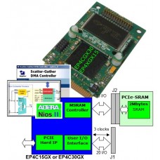
This product has been thought to make available a smart PCI express I/O able to be a powerful front end. It can host at same time the NIOS microcontroller, the Scatter Gather DMA and hardwired logic with DSP blocks.
Its use allows the interfacing of a lots of sensors, converters and actuators with high performance, both in interrupt response, both when is required a high speed data transfer to/from main memory but also when the data must be processed by DSP or NIOS with its custom instructions before that has been sent to the host cpu.
To reduce the number of Fpga I/O pins required to allow the use of the FPGA boards J2, the SRAM board has been designed with a partial multiplexed Address/Data Interface. The user have to interface the SRAM module using a Multiplexed SRAM Controller (MSRAM in the figure) that split 32 bits data access in 2x16 bits data access. To minimize access timing during cache line fill operations, the SRAM LSBits A3-A0 (Avalon A4-A1) addresses bits haven’t been multiplexed.
The GEB Enterprise parameterizable MSRAM controller IP can be used to interface the SRAM module to the Avalon bus. It contains the logic needed to split the Avalon bus 32 bits cycle in one send address cycle (when it’s needed) and two data cycles
Write a review
Your Name:Your Review: Note: HTML is not translated!
Rating: Bad Good
Enter the code in the box below:
GEB-Enterprise-Shop © 2025


