Shopping Cart
0 item(s) - 0.00€PCIE-IOBUS-MS32 (Windows SDK)
Add to Compare
GPIO-BUS MS-Windows 32bits, XP and Seven: PCIe to General Pourpuse I/O Bus Bridge (PCIe target), Drivers, QSYS and Demo Sources
The IOBUS IP is a dynamically reconfigurable asynchronous bus master designed by GEB Enterprise. It supports 8/16/32 Data Bus wide, external interrupts, either fixed latency or variable latency bus cycle.
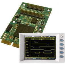
The IOBUS shall be the bus used for communication between a master (the Pcie card) and an unspecified number of slaves. The bus supports up to 32 Data bits, up to 8 bits address, 2 Chip Select (CS#), Read Enable(RD#), Write Strobe (WR#), Interrupt request (INT#) and an optional Wait signal (WAIT#).
The bus cycle timing can be defined by a control register, setup, hold and pulse width can be changed by user allowing bus cycle time from 48ns to 768ns with 16ns steps. Additional delay can be added by WAIT# signal.
The system includes VHDL source, QSYS design, command line demo source and executable, fpga loadable files (both EP4CGX15BF14C7N and EP4CGX30BF14C6N fpga).
Write a review
Your Name:Your Review: Note: HTML is not translated!
Rating: Bad Good
Enter the code in the box below:
GEB-Enterprise-Shop © 2025


